The past 2007 was very successful for the development of many Intel technologies, including in the field of silicon photonics. MIT Technology Review magazine compared Intel's latest breakthrough achievements in this area to a triple win at the races - this is how observers of the leading publication assessed a series of official announcements by the corporation.
According to Justin Rattner, chief technology officer and head of Intel's Corporate Technology Group, “We have empirically demonstrated that manufacturing technologies compatible with CMOS silicon design enable the creation of semiconductor optical devices. Proving this fact was a huge achievement, but no less significant steps are needed for the further development of this technological direction. We now need to learn how to integrate silicon photonics devices into standard computer components; We still don’t know how to do this. But at the same time, we continue to actively work with the divisions involved in the development of various types of products to offer manufacturers models for using semiconductor photonics in Intel solutions.”
Researchers at Intel have developed the world's first semiconductor chip capable of producing high-quality continuous laser beams. Eight lasers are integrated into one silicon chip.
Silicon photonics as a means to eliminate bottlenecks on the road to the era of tera computing
Silicon photonics is a critical component of Corporate Technology Group's long-term development strategy aimed at accelerating the transition to tera computing. The fact is that as multi-core processors with enormous computing power develop, new problems arise for engineers. For example, the demand for communication speed between memory and processor will soon exceed the physical limitations imposed by copper conductors, and the transmission speed of electrical signals will become slower than the speed of the processor. Already, the performance of powerful computing systems is often limited by the speed of data exchange between the processor and memory. Today's data transmission technologies are designed for much lower bandwidth compared to photonics, and as the distance over which data is transmitted increases, the transmission speed becomes even slower.
“It is necessary to bring the data transfer speed between the components of the computing platform in line with the speed of the processors. This is indeed a very important task. We see silicon photonics as a solution to this problem and are pursuing a research program that positions us at the forefront of this field,” said Intel Distinguished Research Engineer Kevin Kahn.
Tests of a prototype optical memory module have shown that light, rather than electricity, can be used to access server memory.
A team led by Intel's lead optics researcher, Drew Alduino, is developing an optical processor-to-memory communication system for Intel platforms. A test platform has already been created based on fully buffered FB-DIMM memory, on which Microsoft Windows boots and runs. The current prototype is proof of the ability to connect memory to the processor using optical communication lines without compromising system performance.
Creating a commercial version of such a solution has enormous benefits for users. Optical communication systems will eliminate the bottleneck between memory bandwidth and processor speed and improve the overall performance of the computing platform.
From research to implementation
The Photonics Technology Lab, led by Intel Distinguished Research Engineer Mario Paniccia, has proven that all optical communications components—laser, modulator, and demodulator—can be manufactured from semiconductors using existing manufacturing technologies. PTL has already demonstrated critical silicon photonics components operating at record-breaking performance, including modulators and demodulators delivering data rates of up to 40 Gbps.
To implement semiconductor photonics technology, six main components are required:
- laser emitting photons;
- a modulator for converting a stream of photons into a stream of information for transmission between elements of the computing platform;
- waveguides, which act as “transmission lines” to deliver photons to their destinations, and multiplexers to combine or separate light signals;
- a case, especially necessary for creating assembly technologies and low-cost solutions that can be used in mass production of PCs;
- a demodulator for receiving streams of photons carrying information and converting them back into a stream of electrons available for processing by a computer;
- electronic circuits to control these components.
%%%
The issue of implementing all these optical communication components using semiconductor technologies is widely recognized as a major research problem, the solution of which will lead to a huge technical breakthrough. PTL has already set a number of world records by developing high-performance devices, modulators, amplifiers and demodulators that provide data rates of up to 40 Gbps. Over the next five years, Intel will look to integrate these components into actual products.
One of the key components of silicon photonics is a modulator that provides transmission speeds of up to 40 Gbit/s.
In the field of semiconductor photonics, Intel has already entered the home stretch. Research in the field of integration of optical elements has already moved from the stage of scientific or technological development to the stage of creating commercial products. The research team is now focused on identifying the capabilities and specifications for designing innovative products based on this revolutionary technology. Ultimately, Intel teams create prototypes and work closely with product development teams to accelerate adoption of new technology.
In addition to its own activities, Intel is funding some of the most promising research in this area outside of CTG - in particular, it is collaborating with the University of California at Santa Barbara, which is developing a hybrid semiconductor laser. Talented graduates from various universities from other countries also undergo internships at the PTL laboratory.
Intel's leading optics researcher, Richard Jones, said: “We are facing two major challenges in the current hybrid semiconductor laser project. First, we must move hybrid laser pilot production from the University of California to the Intel plant. Secondly, we have to combine a hybrid laser, a high-speed semiconductor modulator and a multiplexer to prove that we can create a single optical transmitter based on CMOS-compatible manufacturing technology.”
The introduction of silicon photonics technologies will involve the development of new manufacturing processes for producing lasers at high volume scale. Intel's successes in the field of photonics will allow it to significantly outperform potential competitors. PTL Laboratory has already registered about 150 patents. The most prestigious publications, such as Nature, noted the unprecedented achievements of Intel specialists. Additionally, Intel was awarded the 2007 EE Times ACE Award for Most Promising New Technology.
Chasing photons
Unlike existing well-established transistor production processes that have been proven for decades, the technology for creating elements for semiconductor photonics is completely new. There are certain problems on the way to its implementation: optimizing devices, increasing design reliability, developing test methodology, ensuring energy efficiency, and developing subminiature devices.
Test bench for 40 Gigabit silicon laser modulator
One of the most important problems is optimization, because the PTL laboratory develops optical devices for mass computing. While there are no other similar products, standards or other reference points, engineers developing a new technological process themselves search for solutions that best meet the needs of computer applications.
Currently, a group of researchers from the PTL laboratory, relatively small by photoelectronics standards, is gradually switching to the commercialization of semiconductor photonics solutions and expects that mass adoption of this incredible technology could begin as early as 2010. A group of optics specialists from the Digital Enterprise Group (DEG) under under the leadership of Victor Krutul, it is developing applications that will provide the basis for the development of new technology. "We believe that by mastering optical communications, Intel products will continue to comply with Moore's Law," says Krutal.
When photons, rather than electrons, are used to transfer information between components of the same computing platform and between different systems, the next computer revolution will take place. Leading electronics manufacturers around the world have already joined this race, seeking to gain a competitive advantage. The significance of the new technology can be compared to the invention of integrated circuits. Intel is leading the way in this research and in the development of semiconductor photonics-based components.
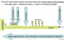
Today, optical connections are used primarily at the device-to-device level or in optical networks. Their main components and operating principles are discussed in one of the previous ones. However, there are three other categories of interconnects—board-to-board, chip-to-chip, and in-circuit communications—for which the main difficulty in implementing optical interconnects lies in the need to combine optical and electronic functions on a common semiconductor substrate. This problem may be solved by silicon photonics, which uses silicon-based materials to generate, transmit, control and detect light.
Reasons
Interest in the development of optical communication channels at the board level was caused by the creation of blade servers. The obvious target for optical technology here is the backplane. It typically supports high-speed point-to-point or multipoint connections with typical lengths of up to 1 m. Key benefits of optical patch panels include low crosstalk and high bandwidth. However, many of today's optical patch panels are more like patch panels. They demonstrated a range of optical technologies, including polymer silicon fibers, ribbon fibers integrated with vertical cavity surface emitting lasers (VCSELs), planar fiber chains, and photodiodes. But none of them, with the exception of some niche applications, have replaced copper connections.
It is difficult to predict whether the clock speed race in the processor industry will stop, because extrapolating from Moore's law, we can expect the appearance of chips with clock frequencies of about 10 GHz by the end of 2010. However, even at current frequencies, it is becoming increasingly difficult to provide the required bandwidth in printed circuit boards or modules based on copper buses. Loss on copper FR-4 (Flame Resistance 4) PCBs has been shown to increase rapidly at frequencies above 1 GHz, with signal-to-noise ratios deteriorating and timing errors occurring. In addition, crosstalk limits wiring density. High-speed optical channels up to 10 cm long between microcircuits have a number of advantages compared to copper ones. They have lower losses with greater bandwidth, and are not subject to electromagnetic crosstalk. In the last 20 years, optical technologies have been proposed to overcome the limitations of copper wiring, but the relatively high cost and use of exotic materials have made them unsuitable for large-scale production.
Designing electrical connections within integrated circuits operating at multi-gigahertz frequencies is also becoming increasingly complex. In such a situation, optical channels with a typical length of less than 1 cm become potentially attractive. The following reasons contribute to this:
- reduction of delay times compared to the use of copper conductors;
- large bandwidth that does not limit the increase in clock frequencies of transistors;
- reduced power consumption;
- insensitivity to electromagnetic interference.
However, today, efforts to integrate optics and electronics are not only in their early stages, but are also quite expensive compared to traditional copper-based technologies.
Intel is conducting very intensive research in this area, whose approach to solving the problem is based on silicon photonics. The main building blocks of the proposed integrated platform here are a tunable External Cavity Laser (ECL), a silicon modulator, a silicon-germanium photodetector, and low-cost interconnect technology.
Silicon light sources
Although silicon-based lasers are not yet achievable, work on such light sources emitting in the visible and infrared ranges is underway widely around the world. Silicon sources are one of the organic parts for monolithic integration, since they allow the fabrication of both optical elements and control electronics on a single substrate. When using silicon light guides, the radiation should be in the infrared range with a wavelength of more than 1.1 microns, since it is in this window that losses are minimal.
Currently, most research is being conducted in the direction of using the effect of electroluminescence - radiation obtained as a result of electrical pumping. Until reliable and efficient silicon emitters are obtained, the possibility of hybrid integration, i.e., the use of non-silicon light sources connected to silicon light guides, is being considered.
The difficulty in manufacturing silicon light sources is caused by the presence of a band gap with indirect transitions. This leads to the fact that the probability of nonradiative transitions (in particular, Auger recombination) becomes higher than those with light emission.
To obtain infrared radiation, appropriate impurities, such as erbium, must be introduced into silicon. Silicon light guides doped with erbium emit in the infrared range if they are additionally doped with oxygen to form optically active ions in the lattice. However, this type of device has a significant drawback: although the radiation intensity is relatively high at 100° K, at room temperatures it drops sharply.
The next way to increase the efficiency of light output in silicon is to reduce the number of nonradiative transitions during electron-hole recombination. This is achieved by reducing the diffusion of carriers to nonradiative recombination centers in the lattice, which increases the probability of light-emitting transitions. One method of such limitation, compatible with VLSI technology, is based on the use of nanocrystals. Other means involve the use of quantum wells in GeSi or crystal lattice defects.
Impurities other than erbium can be included to produce radiation at other wavelengths. For example, terbium provides radiation with wavelengths of 0.98 and 0.54 microns. However, the lifetime and reliability of such devices are too low for practical use.
Another limitation for all types of silicon light sources with direct current is the low direct modulation speed - about 1 MHz. This means that they require external modulators to create high-speed channels.
Device architecture
Work on creating silicon light sources continues, but they are still far from complete. And until a reliable and efficient silicon light source appears, integrated photonics systems will require traditional materials of groups III-V of the periodic table.
Following Intel, we give an example of how an external cavity laser and a silicon light guide with a Bragg grating can be used as a filter for group III-V light generated by the crystal in order to obtain the desired wavelength for optical communications. The strong thermo-optical effect in silicon can be used to tune the generated wave.
The Bragg grating was made by etching a number of 1.2 × 2.3 × 3.4 μm grooves onto a silicon-on-insulator (SOI) wafer. Then, after appropriate processing, the details of which we omit, the Bragg grating was placed in the light guide. The ELC was built by connecting a light guide containing a Bragg grating to an amplifier chip. The resonator was formed between a Bragg grating, serving as a mirror on one side, and an amplifier chip with a 90% reflective coating, forming a mirror on the opposite side. The light guide with the Bragg grating was connected to the amplifier chip at an angle of 8°, which, together with the non-reflective coating, reduced the effective reflectivity of the face to 10-5. The generated beam exited from the side of the laser diode on which a 90% reflective coating was applied and entered the cone of a single-mode optical fiber with a lens (Fig. 1). The lens served to increase the coupling between the optical fiber and the laser. To better understand the operating principle of a laser with an external cavity using a Bragg grating, we present its diagram using more traditional components (Fig. 2).
Silicon modulators
So, above we described a tunable laser based on a complex semiconductor diode of groups III-V and a silicon Bragg grating. However, the laser output produces a continuous wave, which does not carry information. To transmit data over optical communication channels, an optical modulator is required. Such devices with modulation frequencies above 1 GHz were typically made from either ferroelectric lithium niobate crystals (LiNbO3) or complex semiconductors with multiple quantum wells, which exploit the localized Stark effect (splitting of the spectral lines of an atom under the influence of an external electric field) or the electroabsorption effect . The modulation frequency in these devices reaches 40 GHz.
Market demand for low-cost solutions has stimulated the development of silicon-based modulators. In addition, silicon photonics makes it possible to obtain monolithic integrated optical elements based on CMOS technology.
Silicon-based optical modulators have been proposed and demonstrated by many research centers. We present here an experimental version of a device based on a Mach-Zehnder interferometer (MZI). Thanks to the original development of a phase-shifting circuit based on a MOS capacitor built into the MZI passive silicon waveguide, a modulation frequency of 2.5 GHz can be achieved for a wavelength of 1.55 µm.
A schematic representation of the MCI is shown in Fig. 3. The incoming light is split into two equal parts and directed into the two arms of the interferometer. Each of them can contain an active section, which, using an applied voltage, slightly changes the speed of light propagation in the arm. Due to this, a phase shift of the beams is obtained at the output, which, due to interference, leads to intensity fluctuations in the resulting beam.
Silicon photodetectors
The final active component that must be integrated into an all-silicon optical platform is the photodetector. Silicon photodetectors are already widely used for applications using visible light (0.4-0.7 µm), such as in digital cameras and scanners, due to their high efficiency at these wavelengths. However, most semiconductor lasers used in communications operate in the near-infrared region, typically 850, 1310 and 1550 nm, a range in which silicon is transparent and a poor detector. The most common way to increase the output current of silicon photodetectors is to add germanium, which reduces the bandgap and increases the wavelength of the detected light.
In Fig. Figure 4 shows a cross-section of a photodetector based on SiGe light guides developed by Intel. It is made on the same SOI platform as the previously discussed modulator. The SiGe layer is located on top of the silicon bead of the light guide.
The first version of the detector used 18 quantum wells based on Si0.5Ge0.5 as a light-absorbing material. Sensitivity for some devices reached 0.1 A/V at a light wavelength of 1316 nm. The developers believe that with some improvements the sensitivity can be increased to 0.5 A/V. The bandwidth was below 500 MHz due to a significant shift of the valence band, which prevented hole transport. However, it is believed that this drawback can be corrected by changing the composition of the film. Simulations show that throughput can reach 10 Gbps.
Research in the field of silicon-based planar optics has been ongoing in many laboratories around the world for several decades, but industrial samples have not yet been obtained. However, recently there has been significant progress in understanding current problems and possible ways to solve them.
Quantum wells
A quantum well is a potential well that limits the movement of particles. Getting into it, particles that previously moved freely in three-dimensional space can only move in a flat region, essentially two-dimensional. The effect of motion limitation appears when the size of the quantum well becomes comparable to the de Broglie wavelength of the carriers (usually electrons or holes). Let us consider at a qualitative level how a quantum well is created.
As is known, in accordance with band theory, the energy spectrum of a semiconductor consists of three bands (from bottom to top): valence band, band gap band, and conduction band. If a thin layer of a narrow bandgap semiconductor is placed between two layers of wide bandgap semiconductors, then the conduction band electrons of the middle thin layer, which have an energy lower than the energy level of the wide band gaps of the adjacent semiconductors, will not be able to penetrate the potential barrier formed by them. Thus, two heterojunctions restrict the movement of electrons on both sides, i.e., the electrons are locked in one direction. We can say that the movement of electron gas in a quantum well becomes two-dimensional.
Silicon photonics is one of the most promising areas in electronics, which promises a significant reduction in energy consumption and an increase in throughput. This technology allows electro-optical chips to be built on a single silicon chip, allowing individual chips to communicate through optical rather than electrical signals. It took IBM about 12 years to create the first working hybrid chip. The increased performance of systems with such chips makes it possible to create much more powerful supercomputers than those currently in operation.
Thus, the use of light pulses instead of electrical pulses allows for the rapid transfer of very large amounts of information both within one chip and between different parts of an electronic computing system. Previously, the corporation managed to create a photonic transceiver that provided the function of multiplexing channels according to the wavelength of light. Now the company was able to place chips made using silicon photonics technology directly on the processor module. 
Bert Offrein, head of the photonics group at IBM Research - Zurich, together with colleagues from Europe, the USA and Japan, proposes to consider chips made using silicon photonics technology on a par with conventional silicon processors. The technology for manufacturing such chips is also offered as a hybrid one. The team demonstrated the efficient operation of the hybrid chip, which suggests a possible breakthrough in silicon photonics technology. Current designs typically involve the use of an optical transceiver at the edge of the board. But this is not a solution, since the transceiver is located far enough from the processor, and system performance is significantly reduced.

Blue lines are optical fibers that transmit information in the form of light pulses. The orange-yellow structures are copper conductors through which high-speed electrical signals pass. The developers managed to integrate both types of conductors on one chip.
The development of hybrid chips makes it possible to achieve a multiple increase in the performance of the entire system where such chips are used. The development team was able to develop a method for connecting polymer and silicon light guides, despite the fact that the sizes of such structures are very different.

Computer systems with hybrid chips of this type will be used to work with huge amounts of data, which will allow analytical calculations to be carried out, processing data in a matter of seconds. Cognitive computing supersystems can help take technology and science to a new level. But specialists still have a lot of work to do before all this becomes possible.
Photonic logic will not yet replace semiconductor logic, but it can already be used for data transmission. Both between devices and between processor cores.
Looking at the recent announcement of new hardware products from Apple, one would like to say that new technologies are like tropical greenery: just yesterday there was a small stunted shoot, but today there is already a powerful vine that has taken deep roots and firmly embraced the market trunk of computer technology with its shoots.
The appearance of the first Macs with a Thunderbolt interface was greeted with curiosity, but nothing more. Also at one time, the market looked at the outlandish FireWire port in Apple PowerBook 3G laptops.
The subsequent inclusion of Thunderbolt, combined with Display Port, in almost all Apple computing equipment forced peripheral manufacturers to seriously think about supporting this technology. Fortunately, the new controller developed by Intel simultaneously supports both Thunderclap and the USB 3.0 specification. And if everything is clear with the latest interface, then Thunderbolt is full of mysteries. Which ones?
Well, for example, from the series “What’s in your name?” After all, Thunderbolt is the market name for Intel's Light Peak research technology, where the keyword is light. Those ten gigabits per second that Thunderbolt now offers to consumers, transmitting data over copper wires over a distance of up to three meters, are truly flowers in comparison with the fifty gigabits per second that Light Peak provides over an optical cable over a hundred meters.
The appearance of an optical version of Thunderbolt is a matter of the near future. A future in which, along with the microelectronics we are used to, the “queen of light” - photonics - will begin to help process data.
You can read about how Intel uses photonics in its Silicon Photonics Link high-speed data exchange technology in the article “Download in a second: advances in silicon photonics.”
Intel's silicon photonics solutions will provide fifty gigabits per second of computer-peripheral interface bandwidth
It's time to look at the components of silicon photonics-based systems in more detail. Systems, because Intel solutions are far from the only ones. And, most importantly, today these are no longer just laboratory exercises. Silicon photonics has acquired all the necessary capabilities and is quite ready to fruitfully cooperate with existing microelectronic solutions.
An example of such cooperation is the hero of the current material - the IBM project aptly named SNIPER (Silicon Nano-Scale Integrated Photonic and Electronic Transceiver).
Photonics. Bricks of technology
Can photonics completely replace electronics in microcircuitry? Probably not. Light propagation is based on the laws of optics, which imposes significant limitations on the design of basic components such as transistors, capacitors and diodes. No, attempts to develop optical analogues of the transistor were made quite a long time ago, and even today they do not stop. But they cannot compete with proven CMOS technology.
The photonic transistor circuit was proposed back in the eighties of the last century
Where photonics really excels is in implementing high-speed links between digital circuit components. That is, in those places where the electronics begin to slip more and more actively. An increase in the degree of integration of microcircuit components affects the size of the metal conductors connecting them. With the transition to twenty-two nanometer CMOS manufacturing process, engineers were faced with the problem of transient phenomena in miniature copper busbars. These phenomena can easily lead to errors in the operation of a complex computing system tightly packed into a silicon chip.
The use of photonics as a communication medium for microcircuits allows technologists to simultaneously rid new chips of the influence of transient processes in copper conductors and significantly reduce the heating of the microcircuit. Unlike electrons, which unproductively convert their energy into heat, photons, moving along an optical conductor, do not dissipate heat at all.
So, the compromise solution is a combination of electronics and photonics. Electronics retains the basis of digital circuitry, and photonics takes on the role of a universal conducting medium.
What is needed for such an environment? First of all, the source of photons is a laser. Next is the conducting medium through which photons can propagate inside the microcircuits - waveguides. In order for the zeros and ones formed by electronic components to turn into a light flux, and for the inverse conversion, modulators and demodulators will be required, but, of course, not simple ones, but optical ones.
Well, in order to achieve the high throughput required by the channels of current integrated circuits, multiplexers and demultiplexers (also, of course, optical) will be required. Moreover, all these components must be implemented on the same silicon base that is used for CMOS technology.
The development of these “building blocks” is the path that silicon photonics has followed for the last twenty years. During this time, a lot of unique solutions were proposed, which were the very “sum of technologies” that allowed photonics to move to a qualitatively new level. Level of integrated optical-electronic circuits.
Silicon lasers
Actually, the phrase “silicon laser” is an oxymoron. Being a so-called indirect gap semiconductor, silicon is completely incapable of emitting light. This is why fiber optic telecommunications uses solutions based on other (direct gap) semiconductors, such as gallium arsenide. At the same time, silicon is excellent for creating waveguides and detecting optical signals into electrical ones.
So what's the problem? You can use a laser external to the silicon circuit or develop a hybrid circuit based on silicon and, for example, gallium arsenide. But neither solution can be considered effective. In the case of using an external laser (and in modern macro-level fiber-optic systems this is done), at the micro level it is almost impossible to accurately calibrate the beam in relation to a nanometer-sized waveguide. The inclusion of gallium arsenide in the manufacturing process of CMOS chips failed. These two semiconductors require very different production conditions.
So, will a silicon laser never see (or rather emit) light? Of course not. Silicon can be made to glow by using various tricks. For example, doping it with a material that will emit photons beyond the silicon. Or change the structure of the silicon itself in such a way that it will be forced to light up. The third way is to use Raman scattering (also called Raman scattering), which temporarily transforms silicon into an almost direct-gap semiconductor.
One way to make silicon glow is to create a porous silicon structure
Schematic and micrograph of a Raman laser
Currently, scientists have achieved the greatest success in the field of silicon doping technologies. The most famous implementation of a continuous-wave silicon laser based on them is the laser developed by Intel in collaboration with the University of California, Santa Barbara. Scientists managed to “glue” a direct-gap semiconductor indium phosphide to a silicon waveguide using oxide. The thickness of the “glue” is only 25 atoms. By creating a potential difference between silicon and indium phosphide (this is called "electrical pumping"), they achieved the formation of photons, which penetrate through the "glue" into the silicon waveguide.
Schematic diagram of a continuous-wave hybrid silicon laser
Based on this scheme, variants of a hybrid silicon laser with different wavelengths (infrared range, transparent to silicon) are created, which makes it possible to implement a multi-channel communication system.
Silicon modulators
The stream of photons emitted by a silicon laser can be thought of as a carrier frequency that needs to be modulated by a binary signal.
Optical modulators were considered impossible until scientists decided to exploit the phenomenon of light interference. In general, a modulated optical signal can be obtained by interference of a reference beam of light and a beam passed through a material that changes the refractive index under the influence of an electric current (the so-called electro-optical effect). Unfortunately, silicon let us down here too - its symmetrical crystal lattice does not allow the electro-optical effect to be realized. Doping came to the rescue again.
The scientists bifurcated the silicon waveguide and built up a layer of silicon nitride on one of its arms, which stretched the silicon crystal lattice. The application of voltage to this section leads to the refraction of light in this arm of the waveguide. At the same time, in the other arm the same flow propagates without distortion.
Microphotograph of a section of the light refraction arm in a Mach-Zehnder modulator
Implementation of the entire Mach-Zehnder modulator and its variants.
The combination of these fluxes at the output results in their interference, and the output flux will be modulated by applying a voltage to the silicon nitride waveguide arm. Scientists did not have to reinvent the wheel. A similar effect is widely used in Mach-Zehnder interferometers. Therefore, silicon modulators and demodulators were named exactly the same.
Silicon multiplexers
Multiple modulated light streams from multiple lasers with different wavelengths can significantly increase the throughput of a communication channel by parallelizing data transmission. But how can these many threads be combined into one? Moreover, in such a way that the resulting total flow at the output can be divided again. This is where multiplexers come to the rescue. Optical, of course.
The idea of an optical multiplexer based on an array of waveguides (AWG)
Micrograph of an AWG multiplexer
Optical multiplexer based on a cascade of Mach-Zehnder modulators
Currently, a technology has been proposed for microminiature multiplexing of light by means of its spectral multiplexing (WDM - Wavelengths Division Multiplexing). Most often, a diffraction structure based on an array of waveguides and mirrors (AWG - Arrayed Waveguide Grating) is used to implement it, in which each light beam moves along its own waveguide, curved in accordance with its wavelength. When these waveguides come together, they give the resulting spectrally densed flux. Another common solution is to use a cascade of Mach-Zehnder modulators already known to us.
IBM SNIPER. Silicon terabit
Solutions in the field of silicon photonics proposed by Intel are aimed at advancing photonic technologies in the field of peripheral device interfaces. The immediate commercial prospect is a fifty-gigabit optical version of the Thunderbolt interface (perhaps by the time of industrial implementation it will be called differently). In the longer term, Intel is considering increasing throughput to two hundred gigabits per second. To say that it is fast is to say nothing: for example, the contents of a DVD disc at this speed can be transferred in one second.
The IBM Research laboratory has set itself exactly the same goal. I set it and achieved it! True, IBM plans to use its terabit not in communication interfaces, but in high-speed buses connecting the cores of a multi-core processor.
Internuclear communication based on silicon photonics
SNIPER project idea from IBM Research (photonic part of the circuit is shown in blue)
The SNIPER project is a practical implementation of the idea of nanophotonics, using the “building blocks” discussed above to create a photonic communication network. This photonic network is integrated on top of a multilayer system-on-chip pie that includes a multiprocessor module and a RAM module. Having outputs to the outside, such a network provides connection of this system on a chip to a high-speed optical data bus connecting the processor with the periphery. The internal waveguide wiring ensures data routing between the cores of the processor module.
Six-channel photonic module of the SNIPER project
The SNIPER project currently boasts the implementation of a six-channel photonic transceiver module using hybrid silicon lasers, Mach-Zehnder modulators and a waveguide array multiplexer. The throughput of each channel of this transceiver is twenty gigabits per second. Fifty of these channels are implemented on a 25 square millimeter substrate, which provides the same terabit of throughput.
Project SNIPER photonic chip delivering terabit throughput
Most importantly, SNIPER is no longer a research project. Libraries of all photonics elements for silicon lithography have been tested for the production cycle. As well as the technique for integrating them with the CMOS logic of the system on a chip.
Where will this solution be applied first? Of course, in supercomputer systems and cloud computing data centers. Where the computing power of electronic circuits is most needed is to exchange data at the speed of light.
However, we can be sure that the expansion of silicon photonics into consumer computing is not far off. It will all start with the interfaces for connecting peripherals, and then, lo and behold, the buses for multi-core solutions will catch up, turning the boring silicon inside our processors into a magical crystal sparkling with all the colors of the spectrum.
The past 2007 was very successful for the development of many Intel technologies, including in the field of silicon photonics. MIT Technology Review magazine compared Intel's latest breakthrough achievements in this area to a triple win at the races - this is how observers of the leading publication assessed a series of official announcements by the corporation. According to Justin Rattner, chief technology officer and head of Intel's Corporate Technology Group, “We have empirically demonstrated that manufacturing technologies compatible with silicon CMOS design technology enable the creation of semiconductor optical devices.
Proving this fact was a huge achievement, but no less significant steps are needed for the further development of this technological direction. We now need to learn how to integrate silicon photonics devices into standard computer components; We still don’t know how to do this. But at the same time, we continue to actively work with the divisions involved in the development of various types of products to offer manufacturers models for using semiconductor photonics in Intel solutions."
Silicon photonics as a means to eliminate bottlenecks on the road to the era of tera computing
Silicon photonics is a critical component of Corporate Technology Group's long-term development strategy aimed at accelerating the transition to tera computing. The fact is that as multi-core processors with enormous computing power develop, new problems arise for engineers. For example, the demand for communication speed between memory and processor will soon exceed the physical limitations imposed by copper conductors, and the transmission speed of electrical signals will become slower than the speed of the processor. Already, the performance of powerful computing systems is often limited by the speed of data exchange between the processor and memory. Today's data transmission technologies are designed for much lower bandwidth compared to photonics, and as the distance over which data is transmitted increases, the transmission speed becomes even slower.

Tests of a prototype optical memory module have shown that light, rather than electricity, can be used to access server memory
"We need to match the speed of data transfer between components of the computing platform to the speed of the processors. This is really a very important task. We see silicon photonics as a solution to this problem, and therefore we have a research program that allows us to occupy a leading position in this field." , said Kevin Kahn, Distinguished Research Engineer at Intel Corporation.
A team led by Intel's lead optics researcher, Drew Alduino, is developing an optical processor-to-memory communication system for Intel platforms. A test platform has already been created based on fully buffered FB-DIMM memory, on which Microsoft Windows boots and runs. The current prototype is proof of the ability to connect memory to the processor using optical communication lines without compromising system performance.
Creating a commercial version of such a solution has enormous benefits for users. Optical communication systems will eliminate the bottleneck between memory bandwidth and processor speed and improve the overall performance of the computing platform.
From research to implementation
The Photonics Technology Lab, led by Intel Distinguished Research Engineer Mario Paniccia, has proven that all optical communications components—laser, modulator, and demodulator—can be manufactured from semiconductors using existing manufacturing technologies. PTL has already demonstrated critical silicon photonics components operating at record-breaking performance, including modulators and demodulators delivering data rates of up to 40 Gbps.
To implement semiconductor photonics technology, six main components are required:
- laser emitting photons;
- a modulator for converting a stream of photons into a stream of information for transmission between elements of the computing platform;
- waveguides, which act as "transmission lines" to deliver photons to their destinations, and multiplexers to combine or separate light signals;
- a case, especially necessary for creating assembly technologies and low-cost solutions that can be used in mass production of PCs;
- a demodulator for receiving streams of photons carrying information and converting them back into a stream of electrons, available for processing by a computer;
- electronic circuits to control these components.
The issue of implementing all these optical communication components using semiconductor technologies is widely recognized as a major research problem, the solution of which will lead to a huge technical breakthrough. PTL has already set a number of world records by developing high-performance devices, modulators, amplifiers and demodulators that provide data rates of up to 40 Gbps. Over the next five years, Intel will look to integrate these components into actual products.
In the field of semiconductor photonics, Intel has already entered the home stretch. Research in the field of integration of optical elements has already moved from the stage of scientific or technological development to the stage of creating commercial products. The research team is now focused on identifying the capabilities and specifications for designing innovative products based on this revolutionary technology. Ultimately, Intel teams create prototypes and work closely with product development teams to accelerate adoption of new technology.
In addition to its own activities, Intel is funding some of the most promising research in this area outside of CTG - in particular, it is collaborating with the University of California at Santa Barbara, which is developing a hybrid semiconductor laser. Talented graduates from various universities from other countries also undergo internships at the PTL laboratory.
Intel's lead optics researcher, Richard Jones, said: "We have two major challenges going forward in the hybrid laser project going forward. First, we must move the hybrid laser pilot production facility from UCLA to Intel's plant. “Secondly, we have to combine a hybrid laser, a high-speed semiconductor modulator and a multiplexer to prove that we can create a single optical transmitter based on CMOS-compatible manufacturing technology.”
The introduction of silicon photonics technologies will involve the development of new manufacturing processes for producing lasers at high volume scale. Intel's successes in the field of photonics will allow it to significantly outperform potential competitors. PTL Laboratory has already registered about 150 patents. The most prestigious publications, such as Nature, noted the unprecedented achievements of Intel specialists. Additionally, Intel was awarded the 2007 EE Times ACE Award for Most Promising New Technology.
Chasing photons
Unlike existing well-established transistor production processes that have been proven for decades, the technology for creating elements for semiconductor photonics is completely new. There are certain problems on the way to its implementation: optimizing devices, increasing design reliability, developing test methodology, ensuring energy efficiency, and developing subminiature devices.
For new components to be used in practice, PTL must ensure that the optical components meet the exceptionally high reliability criteria of the computing industry. In the optical industry, stringent reliability standards have been developed over decades. In accordance with them, months of testing are required before the start of mass production of new products. If problems are identified during these lengthy tests, correcting them and retesting can significantly delay the product's time to market.
One of the most important problems is optimization, because the PTL laboratory develops optical devices for mass computing. While there are no other similar products, standards or other reference points, engineers developing a new technological process themselves search for solutions that best meet the needs of computer applications.
Currently, the PTL research group, relatively small by photoelectronics standards, is gradually shifting its focus to commercializing semiconductor photonics solutions and expects mass adoption of this incredible technology to begin as early as 2010.
A group of optics specialists from the Digital Enterprise Group (DEG), led by Victor Krutul, is developing applications that will provide the basis for the development of new technology. "We believe that by mastering optical communications, Intel products will continue to comply with Moore's Law," says Krutal.
When photons, rather than electrons, are used to transfer information between components of the same computing platform and between different systems, the next computer revolution will take place. Leading electronics manufacturers around the world have already joined this race, seeking to gain a competitive advantage. The significance of the new technology can be compared to the invention of integrated circuits. Intel is leading the way in this research and in the development of semiconductor photonics-based components.


How to make a bag from craft paper with your own hands
Selling modular paintings - affiliate program Affiliate program for selling modular paintings
Important nuances on how to hang an icon in the bedroom, rooms or kitchen
How to choose the right offer in CPA marketing Now let’s look at competitiveness...
Construction affiliate program Your own builder